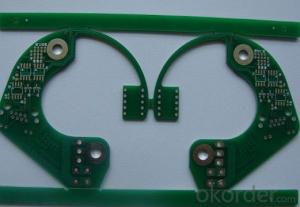
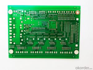
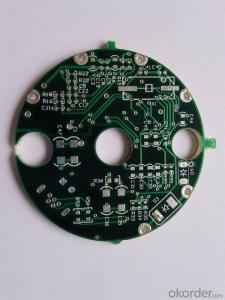
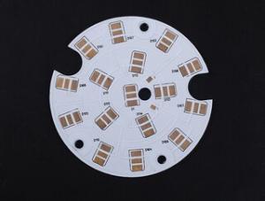
• PCB fab 2-20 layers System 1
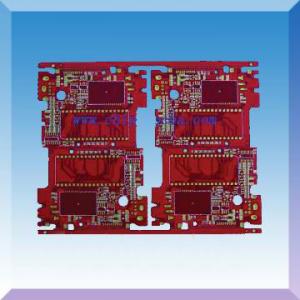
  • PCB fab 2-20 layers System 2
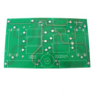
  • PCB fab 2-20 layers System 3
PCB fab 2-20 layers

PCB fab 2-20 layers

Ref Price:
get latest price
Loading Port:
Qingdao
Payment Terms:
TT OR LC
Min Order Qty:
-
Supply Capability:
-

Add to My Favorites

Follow us:


OKorder Service Pledge

Quality Product, Order Online Tracking, Timely Delivery

OKorder Financial Service

Credit Rating, Credit Services, Credit Purchasing

Quick Details

  • Place of Origin: Hebei, China (Mainland)

  • Brand Name: OEM

  • Model Number: customized

  • Number of Layers: 1-32

  • Base Material: FR4 CEM-9 Rogers HF

  • Copper Thickness: 0.5-5 OZ

  • Board Thickness: 0.2-6.0mm

  • Min. Hole Size: 0.2mm

  • Min. Line Width: 4mil

  • Min. Line Spacing: 4mil

  • Surface Finishing: hal immersion gold immersion silver OSP

  • color: red ,green ,yellow, black, white

Packaging & Delivery

Packaging Details:vaccum / anti-static in carton or as your requirement
Delivery Detail:within 20 days after getting your payment

Specifications

electronic test PCB
a. PCB OEM&ODM
b. PCB Clone/Copy,Design
d. Turnkey service
e. UL,SGS,RoSH,TS certificate

 PCB Manufacturer

OurPCB Technical capabilities

NO

ITEM

Technical capabilities

1

Layers

2-20 layers

2

Max. Board size

2000×610mm

3

Min. board Thickness

2-layer  0.15mm

4-layer  0.38mm

6-layer  0.55mm

8-layer  0.80mm

10-layer  1.0mm

4

Min. line Width/Space

0.075mm(3mil)

5

Max. Copper thickness

6OZ

6

Min. S/M Pitch

0.075mm(3mil)

7

Min. hole size

0.1mm(4mil)

8

Hole dia. Tolerance (PTH)

±0.05mm(2mil)

9

Hole dia. Tolerance (NPTH)

+0/-0.05mm(2mil)

10

Hole position deviation

±0.05mm(2mil)

11

Outline tolerance

±0.10mm(4mil)

12

Twist & Bent

0.75%

13

Insulation Resistance

>1012 Ω Normal

14

Electric strength

>1.3kv/mm

15

S/M abrasion

>6H

16

Thermal stress

288°C 20Sec

17

Test Voltage

50-300V

18

Min. blind/buried via

0.15mm  (6mil)

19

Surface Finished

HAL, ENIG, ImAg, Imsn OSP, Plating AG, Plating gold

20

Materials

FR4,H-TG,Teflon,Rogers,Ceramics,Aluminium, Copper base


Q:What are the single panel needs to be tested?
Anti - - in welding inspection (printing solder layer), text (text printing) - surface treatment (according to the requirements of production, OSP, gold, tin etc.) - molding - Test (electrical measurement, generally using universal test frame, fewer orders can fly test, comparison cost saving)
Q:What does A mean?
According to the circuit board layer to the right is divided into single panel, double sided and multilayer circuit board, the three main categories. The first is a single panel, in the most basic parts of PCB, focused on one side, the wire is concentrated on the other side. Because the wire appears only in one side, so we call this PCB single sided circuit board. The single panel usually has the advantages of simple manufacture, low cost, but the drawback is not applied to too complex products.
Q:Printed circuit board, double-sided printing or single-sided printing? What is the difference?
Double good,it is necessary to use a double-sided board. Both sides of the copper covered with a line, and through the hole to pass through the two layers of the line, so that the formation of the required network connection.
Q:Circuit board production process is what?
After the formation of the interlayer conducting hole, the metal copper layer is needed to be arranged on the interlayer to complete the conduction of the interlayer circuit. In severe and high pressure washing brush grinding way to clean dust and lint holes on the then Potassium Permanganate solution for removing rubber residue on the surface of the hole wall copper. Soak up the tin and palladium colloid layer on the clean hole wall, and then restore it to palladium. The circuit board is immersed in a chemical copper solution, and the copper ions in the solution are reduced and deposited on the hole wall by the catalysis of palladium metal to form a through hole circuit. The copper layer in the through hole is thickened to resist the thickness of the subsequent processing and the impact of the environment in the way of the copper plating bath.
Q:What is the reason for the short circuit of a single board patch?
Patch before the short circuit
Q:I encountered in the repair process two panel IC replacement. It is difficult to remove the circuit board IC. Disconnect the circuit board is broken, really let me headache. Trouble you tell the younger brother how to dismantle, choose the kind of electric iron good? Is there a good way? Not with a needle
Circuit board, also known as circuit board, PCB board, aluminum substrate, high frequency board, ultra-thin circuit board, ultra-thin circuit board, printing (copper etching technology) circuit board, etc..
Q:What is the best PCB circuit board
Common multilayer board is generally 4 or 6 layers of plywood, complex multilayer board up to ten layers. So, here's a brief introduction. A single panel single panel (Single-SidedBoards) on the most basic PCB, the parts are concentrated in one side, the wire is concentrated on the other side. The PCB is called a single panel (Single-sided) because the wire only appears on one side.
Q:Single-sided circuit board generally have those types, and how to separate?
Details are as follows: 94HB: ordinary cardboard, not fire (the most low-grade materials, die punch, can not do power board). 94V0: flame retardant paper board. 22F: single side half glass fiber board (die punching). CEM-1: single side glass fiber board (must be computer drilling, can not punch). CEM-3: double sided glass fiber board (in addition to the double sided board is the lowest side of the plate material, a simple double-sided board can use this material, cheaper than FR-4 will be 5~10 yuan / square meter). FR-4: double glass fiber board.
Q:After the circuit board is a double - coated copper or a single side of the copper cover good?
The so-called copper cover, is on the PCB idle space as the reference surface, and then filled with solid copper, copper is also known as copper. The significance of copper coating is to reduce the ground resistance and improve the anti-jamming ability
Q:What does PCB mean?
Because it is made of electronic printing, it is called "printed" circuit board.

1. Manufacturer Overview

Location
Year Established
Annual Output Value
Main Markets
Company Certifications

2. Manufacturer Certificates

a) Certification Name  
Range  
Reference  
Validity Period  

3. Manufacturer Capability

a)Trade Capacity  
Nearest Port
Export Percentage
No.of Employees in Trade Department
Language Spoken:
b)Factory Information  
Factory Size:
No. of Production Lines
Contract Manufacturing
Product Price Range

Send your message to us

This is not what you are looking for? Post Buying Request

Similar products

New products

Hot products


Hot Searches